- 您现在的位置:买卖IC网 > Sheet目录1996 > ICS570GI-01T (IDT, Integrated Device Technology Inc)IC MULTIPLIER/ZDB 8-MSOP
ICS557-01
PCI-EXPRESS GEN1 CLOCK SOURCE
PCIE
IDT PCI-EXPRESS GEN1 CLOCK SOURCE
4
ICS557-01
REV P 072512
PCI-Express Layout Guidelines
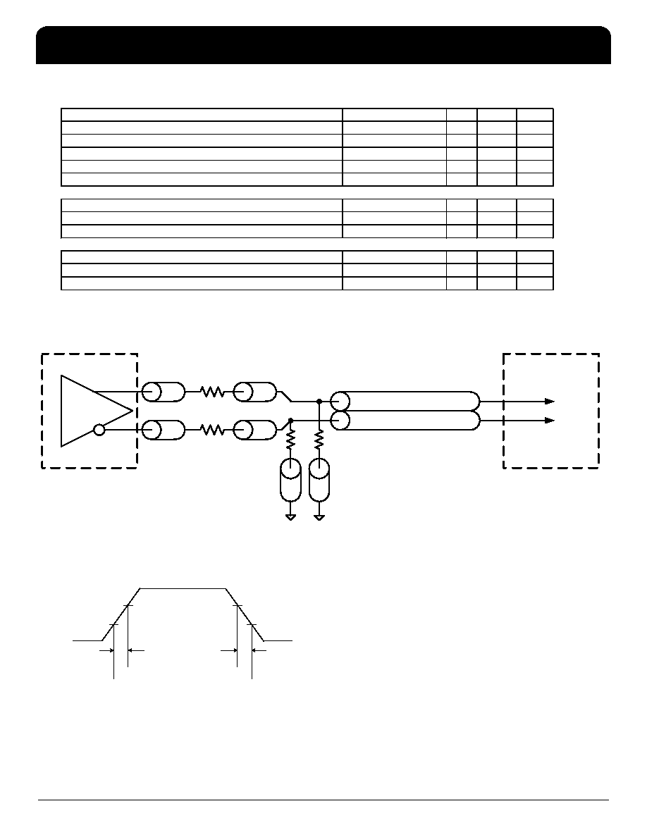
Figure 1: PCI-Express Device Routing
Typical PCI-Express (HCSL) Waveform
Common Recommendations for Differential Routing
Dimension or Value
Unit
Figure
Notes
L1 length, Route as non-coupled 50 ohm trace.
0.5 max
inch
1,2
L2 length, Route as non-coupled 50 ohm trace.
0.2 max
inch
1,2
L3 length, Route as non-coupled 50 ohm trace.
0.2 max
inch
1,2
RS
33
ohm
1,2
RT
49.9
ohm
1,2
Differential Routing on a Single PCB
Dimension or Value
Unit
Figure
Notes
L4 length, Route as coupled microstrip 100 ohm differential trace.
2 min to 16 max
inch
1
L4 length, Route as coupled stripline 100 ohm differential trace.
1.8 min to 14.4 max
inch
1
Differential Routing to a PCI Express Connector
Dimension or Value
Unit
Figure
Notes
L4 length, Route as coupled microstrip 100 ohm differential trace.
0.25 to 14 max
inch
2
L4 length, Route as coupled stripline 100 ohm differential trace.
0.225 min to 12.6 max
inch
2
R
S
R
S
R
T
R
T
PCI-Express
Load or
Connector
L1
L2
L3’
L4
L1’
L2’
L3
L4’
ICS557-01
Output
Clock
0.175 V
0.52 V
0.175 V
0.52 V
t
OR
t
OF
500 ps
700 mV
0
发布紧急采购,3分钟左右您将得到回复。
相关PDF资料
ICS571MLFT
IC BUFFER ZD LOW PH/NOISE 8-SOIC
ICS601G-01LF
IC CLK MULTIPLIER 16-TSSOP
ICS601M-02ILFT
IC CLOCK MULTIPLIER 16-SOIC
ICS601R-25ILF
IC CLOCK MULTIPLIER 1:5 20-SSOP
ICS613MLF
IC CLOCK MULT LOW PHASE 16-SOIC
ICS650G-40ALFT
IC CLOCK ETHERNET SWITCH 16TSSOP
ICS650GI-44LF
IC CLK SYNTHESIZER 16-TSSOP
ICS650GI-47LF
IC CLK SYNTHESIZER 16-TSSOP
相关代理商/技术参数
ICS570M
制造商:ICS 制造商全称:ICS 功能描述:Multiplier and Zero Delay Buffer
ICS570MI
制造商:ICS 制造商全称:ICS 功能描述:Multiplier and Zero Delay Buffer
ICS570MIT
制造商:ICS 制造商全称:ICS 功能描述:Multiplier and Zero Delay Buffer
ICS570MT
制造商:ICS 制造商全称:ICS 功能描述:Multiplier and Zero Delay Buffer
ICS571
制造商:ICS 制造商全称:ICS 功能描述:Low Phase Noise Zero Delay Buffer
ICS571M
功能描述:IC MULTIPLIER/ZDB 8-SOIC RoHS:否 类别:集成电路 (IC) >> 时钟/计时 - 时钟发生器,PLL,频率合成器 系列:ClockBlocks™ 产品变化通告:Product Discontinuation 04/May/2011 标准包装:96 系列:- 类型:时钟倍频器,零延迟缓冲器 PLL:带旁路 输入:LVTTL 输出:LVTTL 电路数:1 比率 - 输入:输出:1:8 差分 - 输入:输出:无/无 频率 - 最大:133.3MHz 除法器/乘法器:是/无 电源电压:3 V ~ 3.6 V 工作温度:0°C ~ 70°C 安装类型:表面贴装 封装/外壳:16-TSSOP(0.173",4.40mm 宽) 供应商设备封装:16-TSSOP 包装:管件 其它名称:23S08-5HPGG
ICS571MLF
功能描述:IC ZDB LOW PHASE NOISE 8-SOIC RoHS:是 类别:集成电路 (IC) >> 时钟/计时 - 时钟发生器,PLL,频率合成器 系列:ClockBlocks™ 标准包装:2,000 系列:- 类型:PLL 频率合成器 PLL:是 输入:晶体 输出:时钟 电路数:1 比率 - 输入:输出:1:1 差分 - 输入:输出:无/无 频率 - 最大:1GHz 除法器/乘法器:是/无 电源电压:4.5 V ~ 5.5 V 工作温度:-20°C ~ 85°C 安装类型:表面贴装 封装/外壳:16-LSSOP(0.175",4.40mm 宽) 供应商设备封装:16-SSOP 包装:带卷 (TR) 其它名称:NJW1504V-TE1-NDNJW1504V-TE1TR
ICS571MLFT
功能描述:IC BUFFER ZD LOW PH/NOISE 8-SOIC RoHS:是 类别:集成电路 (IC) >> 时钟/计时 - 时钟发生器,PLL,频率合成器 系列:ClockBlocks™ 标准包装:2,000 系列:- 类型:PLL 时钟发生器 PLL:带旁路 输入:LVCMOS,LVPECL 输出:LVCMOS 电路数:1 比率 - 输入:输出:2:11 差分 - 输入:输出:是/无 频率 - 最大:240MHz 除法器/乘法器:是/无 电源电压:3.135 V ~ 3.465 V 工作温度:0°C ~ 70°C 安装类型:表面贴装 封装/外壳:32-LQFP 供应商设备封装:32-TQFP(7x7) 包装:带卷 (TR)